From polysilicon to a packed pallet: the main steps of ingot, wafer, cell and module production, and the materials and checks that decide quality at each stage.
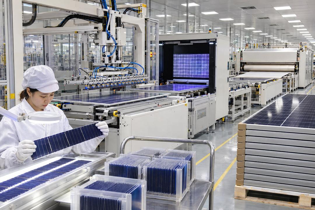
A solar module looks simple from the outside: a sheet of glass, a grid of blue or black cells, an aluminium frame and a small box on the back. Behind it sits a long industrial chain, usually split between specialised factories: polysilicon, ingots and wafers, cells, and finally module assembly. Knowing what happens at each step helps buyers judge quality and helps assemblers decide which materials to source and which checks to insist on.
It starts with polysilicon. Metallurgical silicon is converted to trichlorosilane, purified by distillation and deposited as ultra-pure silicon rods in Siemens reactors; granular silicon from fluidised-bed reactors is a growing alternative. For N-type cells the material must reach around 11N purity, because even parts-per-billion levels of metals or unwanted dopants shorten carrier lifetime in the finished cell.
The polysilicon is melted in a quartz crucible and pulled into a single-crystal ingot by the Czochralski method, with phosphorus added to make it N-type. The round ingot is cropped and squared, then sliced with diamond wire into wafers about 130 µm thick. Today's formats are M10 (182.2 × 183.75 mm), the rectangular G12R (182.2 × 210 mm) and the full-square G12 (210 × 210 mm). Wafers are cleaned, inspected for thickness, chips and saw marks, and packed for the cell plant.
Cell production turns a wafer into a working diode. Texturing etches microscopic pyramids into the surface to trap light. Diffusion or deposition forms the junction: for TOPCon, a boron emitter on the front and a tunnel oxide with doped polysilicon on the rear. Passivation layers of aluminium oxide and silicon nitride reduce surface losses and act as anti-reflective coatings. Screen printing applies silver paste fingers and busbars, and a fast firing furnace sinters them through the coatings to make contact; heterojunction cells skip high-temperature steps and use low-temperature paste instead. Every cell is then flash-tested and sorted into efficiency and colour bins.
Module assembly begins at the tabber-stringer, which solders interconnect wire across the cells to form strings, or lays fine wire on 0BB cells. On the layup line the stack is built from the front: glass, a layer of encapsulant (EVA, POE or EPE), the strings, the bus ribbons that join them, a second encapsulant layer, and finally a rear glass or backsheet. Insulation strips go under bus ribbons, and the ribbon ends are fed through the rear cover for the junction box. Before the stack is sealed, an electroluminescence (EL) image reveals cracks, broken fingers or poor solder joints while repair is still possible.
Lamination fuses the stack into one unit. In a vacuum laminator the air is removed to prevent bubbles, a silicone membrane presses the layers, and the encapsulant melts and cross-links at about 145–150 °C over a cycle of roughly 10–20 minutes, depending on the film. PTFE release cloth keeps squeezed-out material off the equipment. Afterwards, operators check gel content on samples and inspect for bubbles, shifted strings or foreign matter.
Finishing follows. Excess encapsulant is trimmed from the edges, and the frame is fitted, with silicone sealant or tape in the frame groove and corner keys pressed in. The junction box is bonded with silicone, the ribbons are soldered to its terminals, and the box is filled with potting silicone. Modules then rest in a curing area so the sealant and potting can cure before handling.
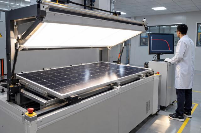
Final testing confirms what the module will deliver. A solar simulator measures the IV curve at standard test conditions (1,000 W/m², 25 °C cell temperature), giving the rated power, voltage and current printed on the label. A second EL inspection catches damage from lamination or framing, and hi-pot and insulation tests check electrical safety. Modules are binned by power, usually in 5 W steps, and labelled.
The last step is packing: corner protectors on each module, 33–36 modules standing on edge in a carton on an ISPM 15 pallet, strapped and wrapped for the container. Good packing is part of quality, because micro-cracks caused in transit are invisible until a field EL test or a drop in yield reveals them. For assemblers, every step above depends on materials that match each other: wafer and cell format, ribbon and stringer, encapsulant and cell type, glass and frame. Sourcing them as a coordinated set makes the line easier to run and the product more consistent.
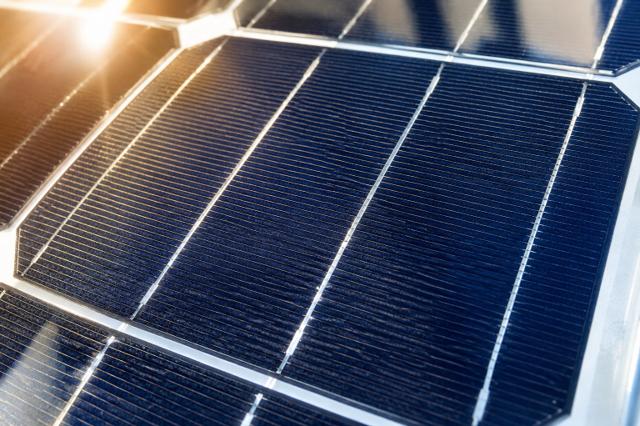
From photon to kilowatt-hour: the physics of a solar cell and the path of energy through a complete PV system.
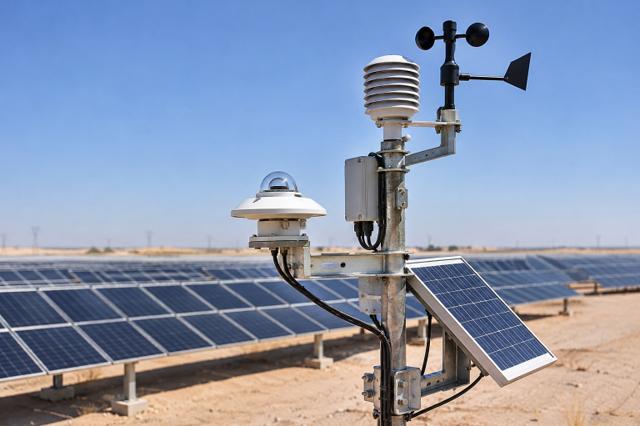
GHI, DNI and DHI explained, how sun position changes through the day and year, and why the Gulf is one of the world's best solar resources.
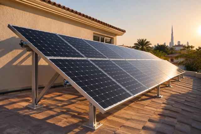
How to orient a PV array: the latitude rule of thumb, why lower tilts often win in the Gulf, and how east–west layouts trade yield for density.
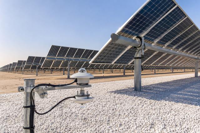
How bifacial modules harvest reflected light, what albedo values to expect on sand, gravel and white membranes, and why bifacial pairs so well with trackers.
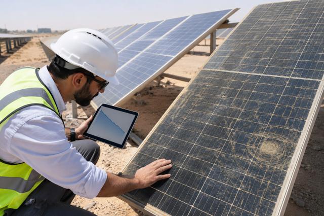
LID, LeTID and long-term power loss explained, and how to read a 12-year product / 30-year linear power warranty.
What the datasheet power really means, how temperature coefficients translate into lost watts, and why heat is the main derating factor in the desert.
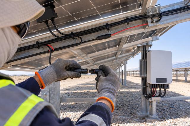
How many modules can go in one string: the cold-temperature Voc limit, the MPPT window and current limits, with a worked 1,500 V example.
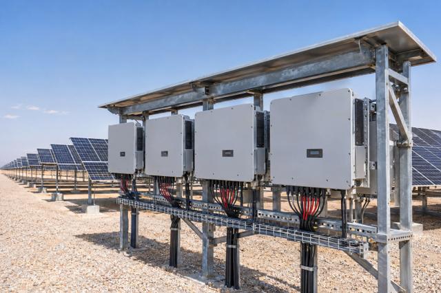
Why PV plants are built with more module power than inverter power, and how to choose a DC/AC ratio between 1.1 and 1.35 without losing too much energy to clipping.
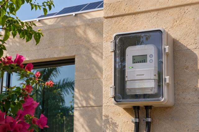
How grid-connected rooftop systems are credited for the electricity they export, and how the tariff scheme changes the right system size and the payback period.

The single number used to compare power plants: lifetime cost divided by lifetime energy, both discounted. What drives it, and why Gulf solar tariffs are among the lowest in the world.
