Blue, multi-grain silicon modules that dominated until about 2018, now discontinued by Tier-1 makers.
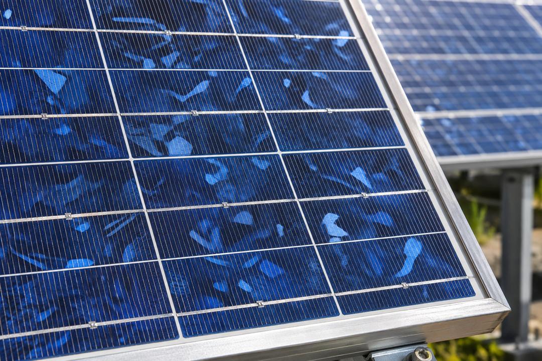
Polycrystalline (multicrystalline) wafers are cut from silicon cast in large blocks, which solidify into many crystal grains. The grain boundaries give the characteristic speckled blue look and act as recombination sites that limit efficiency.
Poly modules typically achieved 15–17 % efficiency with 60- or 72-cell formats of 270–340 W and temperature coefficients around −0.40 %/°C. They were cheaper to make than mono until diamond-wire sawing and Czochralski process improvements erased the cost gap around 2018–2019.
Today all five Tier-1 brands have stopped poly production. Existing plants built with poly modules keep operating, and when repowering or replacing failed modules, designers must check voltage and current compatibility because modern modules are far larger and more powerful.
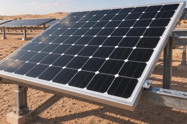
Passivated Emitter and Rear Cell on P-type monocrystalline silicon, the workhorse technology of 2016–2023.
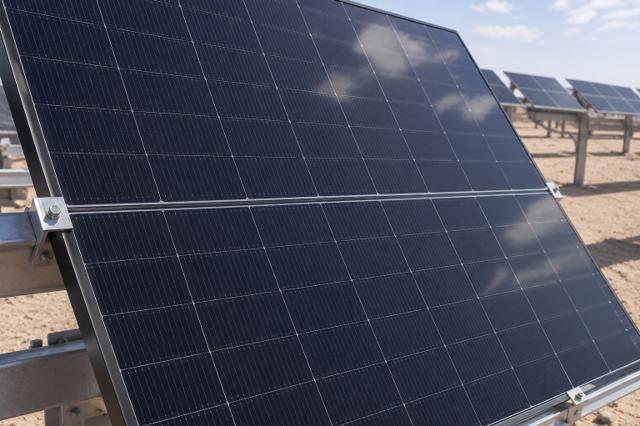
Tunnel Oxide Passivated Contact cells on N-type wafers: today's mainstream high-efficiency, high-bifaciality technology.
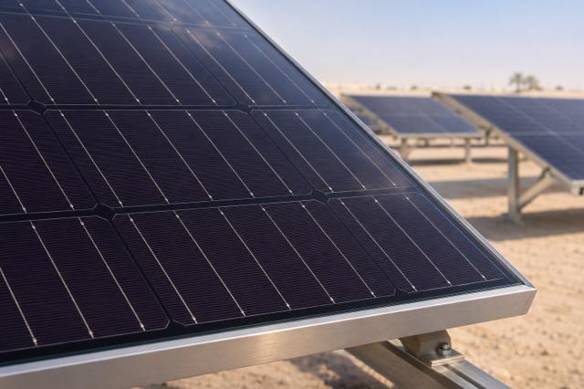
Crystalline N-type wafer sandwiched between thin amorphous-silicon layers, with the best temperature coefficient among silicon technologies.
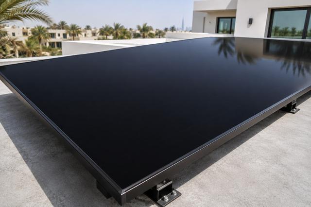
All electrical contacts moved to the rear of the cell. No front busbars, more light captured and the highest module efficiencies on the market.
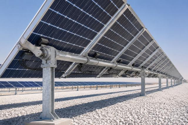
Modules that also convert light reaching their rear side, adding 5–25 % energy depending on ground albedo and mounting height.
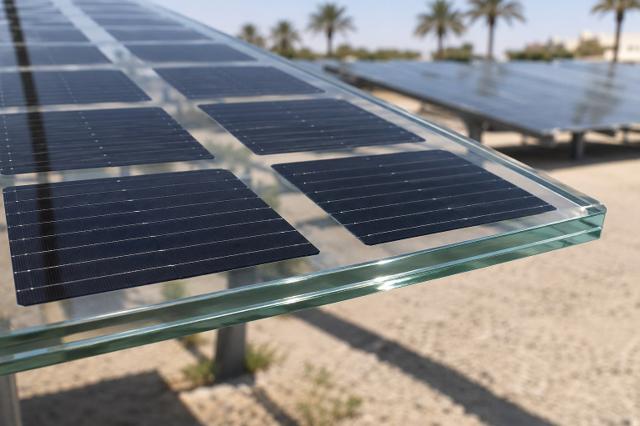
Cells laminated between two sheets of tempered glass for higher durability, lower degradation and 30-year warranties.
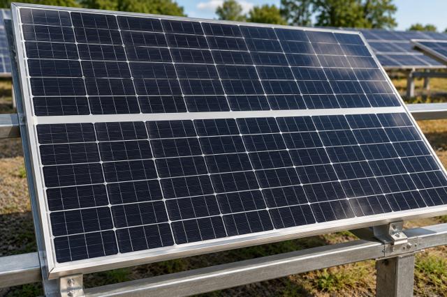
Cells laser-cut in half to halve current per string, reduce resistive losses and improve shade tolerance.
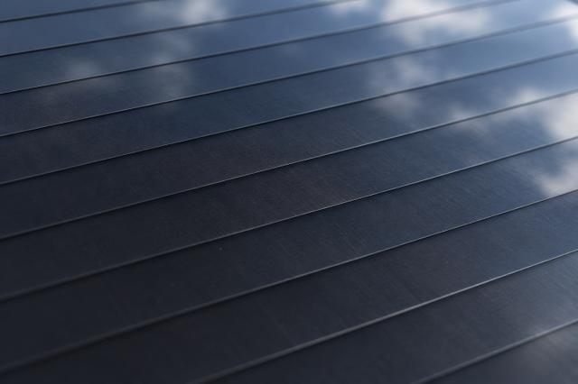
Cell strips overlapped like roof shingles and bonded with conductive adhesive, leaving no gaps or ribbons and a high active area.
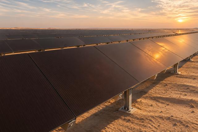
Semiconductor layers a few micrometers thick deposited on glass. Excellent heat and diffuse-light behavior, lower efficiency per area.
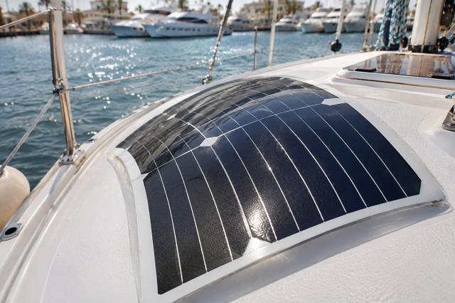
Glass-free laminates for roofs with low load capacity, curved surfaces, vehicles and marine use.
